
Mains voltage does not forgive sloppy engineering. Wiring a $4 development board directly to high-voltage AC without galvanic isolation and proper fail-safe logic is a recipe for catastrophic equipment damage or a workshop fire. The difference between an unstable breadboard prototype and a field-deployable smart power strip comes down to deliberate electrical safety, boot-strapping GPIO discipline, and deterministic firmware states.
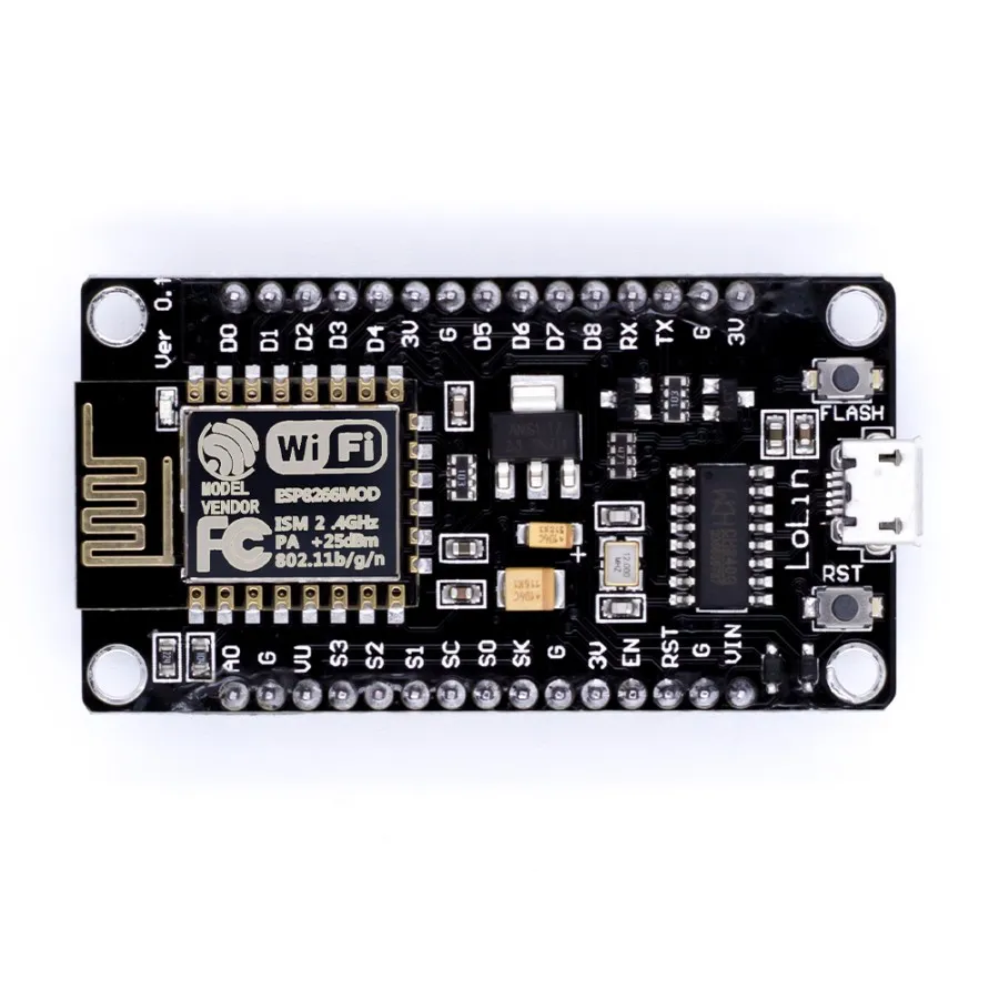
Building a multi-channel Wi-Fi power strip demands strict isolation between the 3.3V logic realm of the NodeMCU ESP8266 and the 250V AC load domain. By coupling an opto-isolated relay array with a cloud backend via Blynk, you achieve low-latency app and voice control while maintaining strict physical and electrical safety barriers.
Hardware Stack and Bill of Materials
Every component in this build serves a distinct architectural purpose. Cutting corners on isolation or interconnects directly degrades your device's safety profile.
| Component | Technical Role | Critical Specification |
|---|---|---|
| NodeMCU ESP8266 | Edge Controller & Wi-Fi Client | ESP8266EX SoC, CP2102/CH340 USB-UART bridge |
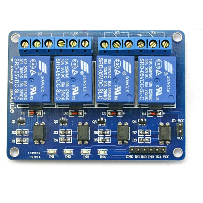
| 4-Channel Relay Module | High-Voltage Galvanic Switching | Active Low, EL817 Optocouplers, Removable JD-VCC Jumper |
| Screw Terminal Blocks | AC Interconnect & Distribution | PCB Mount or DIN Rail rated for mains loads |
| Soldering Station & Solder | Low-Resistance Mechanical Bonding | Sn63/Pb37 Leaded Solder, Temperature-Controlled Iron |
| Blynk IoT Platform | BaaS Control Plane & Transport | Virtual Pin (VPin) Mapping, Cloud WebSocket/MQTT bridge |

Hardware Architecture & Galvanic Isolation
The core design challenge lies in handling the inductive current draw of multiple relay coils alongside high-frequency Wi-Fi transmission bursts without browning out the microcontroller.
1. Power Delivery and the Brownout Trap
A NodeMCU relies on an onboard AMS1117 linear regulator to supply 3.3V to the ESP8266 SoC. Each relay coil consumes roughly 70mA to 80mA when energized. Firing all four channels simultaneously draws over 300mA on the coil side alone. Pair that with the ESP8266's RF transmission spikes reaching ~300mA, and you will exceed standard 500mA USB port limits, crashing the MCU.
To achieve complete galvanic isolation and eliminate brownouts:
- Remove the JD-VCC jumper on the relay board.
- Route clean, dedicated 5V power from an external 5V/2A supply or strong USB-C PD source to JD-VCC and the relay board's ground to energize the coils.
- Connect the NodeMCU 3.3V logic and signal pins to the relay module's VCC and IN1-IN4 input headers.
2. GPIO Pinout and Boot-Strapping Constraints
The ESP8266 features shared internal functions on several pins during power-on reset (POR). Selecting the wrong pin mapping will cause the board to hang or enter programming mode upon boot:
- D1 (GPIO5) & D2 (GPIO4): General-purpose I/O. Ideal for relay control with no boot conflicts.
- D3 (GPIO0): Boot-strapping pin. Must remain pulled HIGH during startup for normal flash boot. Because our relay module is Active Low, keeping the output HIGH during boot satisfies both the hardware boot requirements and holds the relay in a safe de-energized state.
- D4 (GPIO2): Boot-strapping pin tied internally to the onboard LED. Must remain HIGH at boot.
3. Mains Voltage Wiring Discipline
Always disconnect mains power and verify line states with a calibrated multimeter before touching conductors.
- Live (L - Brown/Black): Pass the incoming Live wire into the COM (Common) terminal of each relay channel. Route the NO (Normally Open) terminal to the individual socket load. In this setup, should logic power fail, the spring-loaded contacts disconnect the load immediately (Fail-Safe Default). Avoid using NC (Normally Closed) for safety-critical loads.
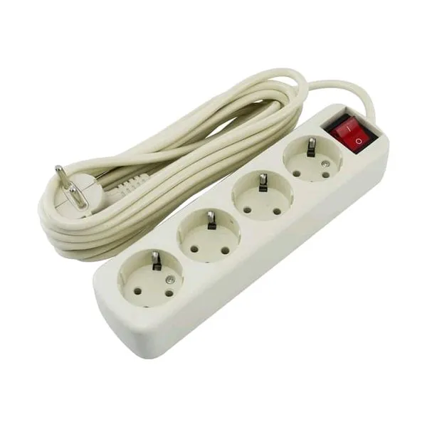
- Neutral (N - Blue/White) & Earth (PE - Green/Yellow): Never switch Neutral or Ground through the relay contacts. Feed them directly across high-capacity terminal blocks to every output outlet.
Production Firmware Architecture
A naive implementation initializes pins after running connection loops, causing connected AC devices to flicker wildly during boot. The firmware below asserts safe HIGH states on all output gates before executing network connections or the Blynk initialization routine.
cpp#define BLYNK_PRINT Serial

#include <ESP8266WiFi.h>
#include <BlynkSimpleEsp8266.h>

// -----------------------------------------------------------------------------
// CONFIGURATION PARAMETERS
// -----------------------------------------------------------------------------
char auth[] = "mWq0GOmizc2NY5-1uY0hPUDhIxxxx"; // Blynk Auth Token
char ssid[] = "lusy";                          // Target Access Point SSID
char pass[] = "lusycantik3";                   // Target Access Point Password

// Relay Channel Mapping
#define RELAY_CH1 D1 // GPIO5
#define RELAY_CH2 D2 // GPIO4
#define RELAY_CH3 D3 // GPIO0 (Strapping Pin: HIGH at boot)
#define RELAY_CH4 D4 // GPIO2 (Strapping Pin: HIGH at boot)

// -----------------------------------------------------------------------------
// BLYNK WRITE HANDLERS (Active Low Switching Logic)
// -----------------------------------------------------------------------------
BLYNK_WRITE(V1) {
  int state = param.asInt();
  digitalWrite(RELAY_CH1, state ? LOW : HIGH);
}

BLYNK_WRITE(V2) {
  int state = param.asInt();
  digitalWrite(RELAY_CH2, state ? LOW : HIGH);
}

BLYNK_WRITE(V3) {
  int state = param.asInt();
  digitalWrite(RELAY_CH3, state ? LOW : HIGH);
}

BLYNK_WRITE(V4) {
  int state = param.asInt();
  digitalWrite(RELAY_CH4, state ? LOW : HIGH);
}

void setup() {
  Serial.begin(9600);
  delay(100);

  // CRITICAL: Force pins HIGH immediately to prevent load chattering during POR
  pinMode(RELAY_CH1, OUTPUT); digitalWrite(RELAY_CH1, HIGH);
  pinMode(RELAY_CH2, OUTPUT); digitalWrite(RELAY_CH2, HIGH);
  pinMode(RELAY_CH3, OUTPUT); digitalWrite(RELAY_CH3, HIGH);
  pinMode(RELAY_CH4, OUTPUT); digitalWrite(RELAY_CH4, HIGH);

  // Network and transport synchronization
  Blynk.begin(auth, ssid, pass);
}

void loop() {
  // Process incoming control frames, manage heartbeats, and run background tasks
  Blynk.run();
}
Control Plane Configuration: Blynk UI
To establish a bidirectional control loop between the physical board and the mobile client:
- Device Setup: Create a new hardware target configured for ESP8266.
- Datastream Definitions: Set up four distinct Datastreams mapped to Virtual Pins V1, V2, V3, and V4 with data types configured as Integer (Range:
0to1). - Widget Instantiation: Add four Switch-style Button widgets to your dashboard canvas. Link each button directly to its corresponding Virtual Pin (V1 through V4).
- Execution Flow: When a user toggles a UI button, the Blynk cloud fires the corresponding
BLYNK_WRITE(Vx)macro, mapping a logical1from the app to an activeLOWtrigger on the optocoupler's input cathode.
Safety, Clearance, and Enclosure Checklist
Operating high-voltage apparatus demands strict adherence to physical safety standards:
- Creepage & Clearance Distances: Maintain a physical clearance gap of at least 3mm between the AC mains traces and low-voltage digital signal traces on the PCB or perfboard. Route physical air slots between relay terminals where possible.
- Overcurrent Protection: Wire a dedicated 10A/250V Thermal Fuse or fast-blow fuse inline with the main AC Live feed prior to feeding the relay distribution rail.
- Enclosure Rating: House the entire assembly inside a non-conductive, UL94-V0 flame-retardant ABS or polycarbonate chassis. Secure all external cable ingress and egress points with industrial strain-relief cable glands.
- Safe Debugging Practices: Never connect a USB debugging cable to your development PC while the mains AC line is live without using a USB isolator.